Imagine rolling your cellphone into a film and clipping it to your pocket like a pen; or folding away your laptop like a newspaper.
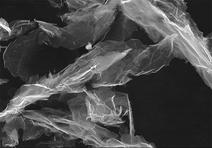
Flakes of carbon atoms knitted in a honeycomb lattice, one atomic layer thick and in theory, infinitely malleable could allow for such a thing.And this material is found in a common pencil.
Graphene was isolated in 2004, by Andre Geim and Konstantin Novoselov at the University of Manchester, resulting in a relatively swift Nobel in 2010. This January,£61m is being funneled into building a ‘National Graphene Institute’ at the university. Set to be operational by early 2015,the five story center is expected to strengthen ties between university research and the factory floor, traditionally lacking in the UK compared to mainland Europe.
As Geim once told the BBC: “It is not even one material. It is a huge range of materials. A good comparison would be to how plastics are used.”And as Novoselov mentioned in his Nobel address: “Although the addition of one layer on top… is all that is needed to arrive at bilayer graphene… this is one of those cases where ‘one plus one is greater than two.’ Bilayer graphene is remarkably different – sometimes even richer in its properties than its monolayer cousin – and fully deserves to be called a different material in its own right.”
Graphene conducts charge 100 times faster than silicon, is waterproof and stretchable, so optimists expect it to upstage silicon. According to the Nobel committee “plastics could be made into electronic conductors if only 1 percent of graphene were mixed into them.”And with “just a fraction of per mille of graphene, the heat resistance of plastics would increase by 30ºC while at the same time making them more mechanically robust.”Grahpene could further boost broadband speeds, create near perfect solar panels, wonder capacitors,and find biomedical applications.
As MIT Technology Review puts it: “There seems little that graphene can’t do.” The challenge: figuring “how to make graphene in large, reliable quantities or how to carve and grow it into the shapes necessary.”Because of another remarkable ability: Graphene can repair itself.
The original discoverers found that displacing a carbon atom from the chain with an electron beam— with others present in the vicinity—resulted in the sheet restoring the original geometry. The disrupted chain also completed itself with metal atoms, but the resulting geometry was distorted. Scientists worldwide are currently using this property to learn to ‘sculpt’ graphene to their advantage; essentially playing with a nano-scale lego set.
Graphene isn’t all about applications. Electrons hurtling through it become massless, achieving speeds comparable to light –providing a far more cost-effective way of studying such phenomenon than a particle accelerator.(In a traditional 3D lattice, this can’t happen because electrons lose energy due to constant collisions, in three directions.) Graphene has also permitted scientists to study another phenomenon priorly confined to theoretical discourse: Klein Tunneling.
In quantum physics, when electrons encounter barriers of higher energy, they have a partial chance of tunneling through.(Imagine a tiny dust speck hurled at a waterfall. The larger the speck, or lesser the gushing water, greater the speck’s chance to reach the other side) In graphene, electron hordes act like the barrier doesn’t even exist. Being massless, electrons in graphene are reflected like light, making it “an excellent material for future energy needs and for quantum computing for enormous calculations while using little energy.” Writes Science Daily.
Unfortunately so far, it’s been located naturally only in outer space. The Spitzer Telescope found graphene in 2011, churned out of collisions in “turbulent stellar winds emanating from planetary nebulae.” It might be too early to start investing in graphene companies as methods of mass manufacture still develop. But in the meantime, China holds the trump card, being the biggest graphite producer, by far.


